17
?2007 Semtech Corp.
www.semtech.com
SC2463
POWER MANAGEMENT
Applications Information (Cont.)
Once the power losses P
loss
for the top (P
t
) and
bottom (P
b
) MOSFETs are known, thermal and package
design at component and system level should be done
to verify that the maximum die junction temperature
(T
j,max
, usually 125
o
C) is not exceeded under the worst-
case condition. The equivalent thermal impedance from
junction to ambient (?/DIV>
ja
) should satisfy
.
P
T
T
loss
max
,
a
max
,
j
ja
d
?/DIV>
?/DIV>
ja
depends on the die to substrate bonding,
packaging material, the thermal contact surface, thermal
compound property, the available effective heat sink
area and the air flow condition (free or forced convection).
Actual temperature measurement of the prototype should
be carried out to verify the thermal design.
Setting the Output V
Setting the Output V
Setting the Output V
Setting the Output V
Setting the Output Volt
olt
olt
olt
oltage
age
age
age
age
The non-inverting input of the channel-one error ampli-
fier is internally tied the 0.5V voltage reference output. A
simple voltage divider (R
o1
at top and R
o2
at bottom) sets
the converter output voltage. The voltage feedback gain
h=0.5/V
o
is related to the divider resistors value as
.
1
2
1
o
o
R
h
h
R
=
Once either R
o1
or R
o2
is chosen, the other can be
calculated for the desired output voltage V
o
. Since the
number of standard resistance values is limited, the
calculated resistance may not be available as a standard
value resistor. As a result, there will be a set error in the
converter output voltage. This non-random error is
caused by the feedback voltage divider ratio. It cannot
be corrected by the feedback loop.
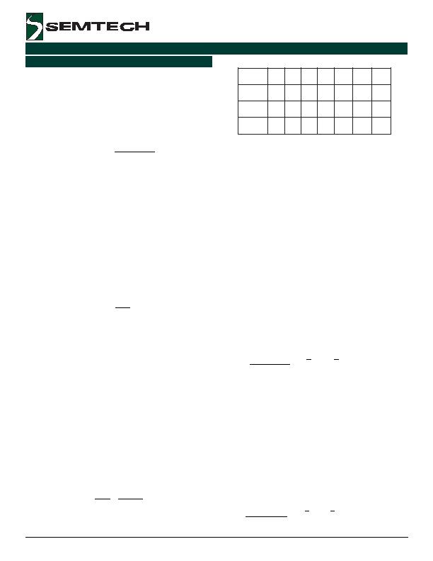
The following table lists a few standard resistor combi-
nations for realizing some commonly used output
voltages.
Only the voltages in boldface can be precisely set with
standard 1% resistors.
From this table, one may also observe that when the
value
5
.
0
5
.
0
1
=
o
V
h
h
)
V
(
o
V
6
.
0 9
.
0 2
.
1 5
.
1 8
.
1 5
.
2 3
.
3
h
/
)
h
-
1
(
2
.
0 8
.
0 4
.
1 2 6
.
2 4 6
.
5
)
m
h
O
(
1
o
R
0
0
2 6
0
8 K
4
.
1 K
2
K
1
6
.
2
K
2
0
.
4
K
2
6
.
5
)
m
h
O
(
2
o
R
K
1 K
1 K
1 K
1 K
1 K
1 K
1
and its multiples fall into the standard resistor value
chart (1%, 5% or so), it is possible to use standard value
resistors to exactly set up the required output voltage
value.
The input bias current of the error amplifier also causes
an error in setting the output voltage. The maximum
inverting input bias currents of error amplifiers 1 or 2 is
200nA. Since the non-inverting input is biased to 0.5V,
the percentage error in the second output voltage will be
100%"(0.2uA) R
01
"R
o2
/[0.5 " (R
o1
+R
o2
) ].
Valley Current Sensing for Current-Limit
Valley Current Sensing for Current-Limit
Valley Current Sensing for Current-Limit
Valley Current Sensing for Current-Limit
Valley Current Sensing for Current-Limit
The valley current sensing for current limiting is a unique
scheme which could sense the voltage across the bot-
tom switch MOSFET when it is on. The scheme is robust
with good noise immunity due to reference to ground.
The current sensing point is at a delay time t
dv
before
the beginning of a switching cycle. Therefore, the actual
valley current is
2
2
)
1
(
_
)
(
?/DIV>
?/DIV>
dv
dv
t
VS
t
L
B
ON
DS
o
V
e
I
e
R
R
V
I
+
+
=
where, I
VS
is the preset valley current limiting threshold.
If a sensed current exceeds the threshold, the top switch
will keep off in the next cycle until the current goes back
below the threshold. In steady state, since the output
voltage is out of regulation in over current condition, the
control loop will try to make maximum duty cycle for the
top switch as it is on, which is usually greater than 80%.
Therefore, as the current falls back below the thresh-
old, it is on in the next almost full cycle. The peak cur-
rent is not controlled and only depends upon circuit pa-
rameters and operating condition in this cycle. The peak
current I
P
is
1
1
)
1
(
_
)
(
?/DIV>
?/DIV>
T
V
T
L
T
ON
DS
o
in
P
e
I
e
R
R
V
V
I
+
+
=
发布紧急采购,3分钟左右您将得到回复。
相关PDF资料
SC338AIMSTRT
IC REG CTRLR DUAL POS ADJ 10MSOP
SC402BMLTRT
IC REG DL BCK/LINEAR SYNC 32MLPQ
SC403MLTRT
IC REG DL BCK/LINEAR SYNC 32MLPQ
SC418ULTRT
IC REG DL BUCK/LINEAR 20MLPQ
SC424MLTRT
IC REG DL BUCK/LINEAR 28MLPQ
SC4250LISTRT
IC HOT SWAP CTRLR 8-SOIC
SC427MLTRT
IC REG DL BUCK/LINEAR 32MLPQ
SE95D,112
IC SENSOR TEMP 2.8-5.5V SOT96-1
相关代理商/技术参数
SC24-681-R
功能描述:INDUCTOR SHIELD 680UH 40MA SMD RoHS:是 类别:电感器,线圈,扼流圈 >> 固定式 系列:SC24 标准包装:500 系列:1331 电感:1.2µH 电流:247mA 电流 - 饱和:247mA 电流 - 温升:- 类型:铁芯体 容差:±10% 屏蔽:屏蔽 DC 电阻(DCR):最大 730 毫欧 Q因子@频率:40 @ 7.9MHz 频率 - 自谐振:130MHz 材料 - 芯体:铁 封装/外壳:0.312" L x 0.115" W x 0.135" H(7.94mm x 2.92mm x 3.43mm) 安装类型:表面贴装 包装:带卷 (TR) 工作温度:-55°C ~ 105°C 频率 - 测试:7.9MHz
SC246B
制造商:Genteq 功能描述: 制造商:GENTEQ / GE 功能描述:
SC246D
制造商:未知厂家 制造商全称:未知厂家 功能描述:TRIAC|400V V(DRM)|10A I(T)RMS|TO-203AA
SC246M
制造商:未知厂家 制造商全称:未知厂家 功能描述:TRIAC|600V V(DRM)|10A I(T)RMS|TO-203AA
SC2475
制造商:SYSTEMSENSOR 制造商全称:SYSTEMSENSOR 功能描述:Strobes and Horn Strobes
SC2475W
制造商:SYSTEMSENSOR 制造商全称:SYSTEMSENSOR 功能描述:Strobes and Horn Strobes
SC2495
制造商:GAMEWELL-FCI 制造商全称:GAMEWELL-FCI 功能描述:SC Strobes and PC Horn/Strobes
SC2495W
制造商:SYSTEMSENSOR 制造商全称:SYSTEMSENSOR 功能描述:Strobes and Horn Strobes